The status quo of semiconductor silicon wafers, more than 90% rely on imports|Semiconductor Industry Observation
In recent years, the proportion of silicon wafers in the semiconductor materials market has basically remained stable, accounting for about 34%. In 2015, the global semiconductor wafer market was approximately US$8 billion, making it the largest IC manufacturing material. Japan’s Shin-Etsu and Sumco account for more than 50% of the sales. Taiwan’s Global Wafer successively acquired Topsil and SunEdisonSemi in 2016, becoming the world’s third largest supplier of semiconductor wafers, and currently the top six wafer fabs With a sales share of 92%, the semiconductor wafer market has been monopolized by giants.
Due to the increase in global shipments of DRAM and 3D NAND Flash in 2016 and the limited production capacity of major international silicon wafer manufacturers, coupled with the failure to ship large-size silicon wafer projects invested by mainland China, the global supply of semiconductor wafers has become tight. The capacity utilization rate of the top several silicon wafer suppliers has reached 100%. The three major semiconductor wafer makers have announced that they will increase the price of 12-inch wafers in Q1 2017 by 10-20%.
According to IC Insights statistics, the number of 12-inch (300mm) fabs in global operations continues to grow, reaching 100 in 2016. By the end of 2020, the total number of 12-inch fabs used in IC production worldwide is expected to reach 117. If 18-inch (450mm) wafers enter mass production, the peak number of 12-inch fabs can reach about 125. Since 12-inch (300mm) silicon wafers are mainly used to produce logic chips and memory chips, and the compound annual growth rate (CAGR) of DRAM and NAND flash memory will reach 7.3% in the next five years, the output value will increase from 77.3 billion U.S. dollars last year. Increased to 109.9 billion US dollars, a growth rate of 42.2%. Therefore, the global demand for large 300mm silicon wafers will continue to expand. It is expected that the shortage of silicon wafers in the next few years will be the norm.
After more than 30 years of vigorous development, the domestic integrated circuit industry has now formed a certain industrial scale, as well as a relatively complete industrial chain pattern supporting the joint development of integrated circuit design, chip manufacturing, packaging and testing and supporting industries. At present, my country’s semiconductor industry is developing rapidly, and the demand for upstream raw materials has maintained this high level. In recent years, the demand for silicon wafers and silicon-based materials has basically been around 13 billion yuan, but 12-inch silicon wafers are totally dependent on imports. In the future, there is a greater possibility of import substitution.
What is a semiconductor wafer
Silicon wafer, also known as silicon wafer, is an important material for the production of integrated circuits. Through photolithography and ion implantation of silicon wafers, integrated circuits and various semiconductor devices can be made. A silicon wafer is a sheet-like object made of silicon, with a diameter of 6 inches, 8 inches, and 12 inches. Monocrystalline silicon is a single crystal of silicon, a relatively active non-metallic element, and has a basically complete lattice structure. Different directions have different properties, and it is a good semiconducting material. The purity is required to reach 99.9999%, or even 99.9999999%, and the impurity content is reduced to the level of 10-9. The Siemens method can be used to prepare high-purity polycrystalline silicon, and then polycrystalline silicon is used as a raw material to grow rod-shaped single crystal silicon from the melt using the Czochralski method or the suspension zone melting method. Monocrystalline silicon wafers are mainly divided into 6 inches, 8 inches, 12 inches and 18 inches according to their diameters.
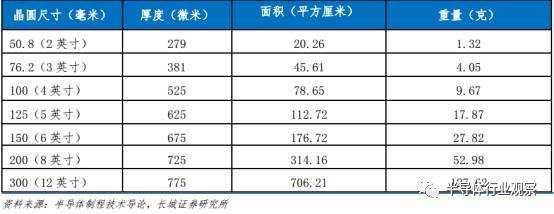
Silicon (Si) is currently the most important semiconductor material, and more than 95% of the world's semiconductor chips and devices are produced using silicon wafers as the base functional material. In the foreseeable future, no other materials (such as graphene, etc.) can replace silicon. Various sizes and specifications of silicon wafers are widely used in the semiconductor manufacturing industry, usually including 4 inches, 5 inches, 6 inches, 8 inches and 12 inches. Their basic specifications are shown in the following table:
Comparison of Czochralski Method and Zone Melting Method
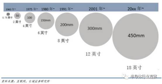
The larger the size of the silicon wafer, the more chips can be cut on each wafer produced in the future, and the cost per chip will be lower. In 1960, there were monocrystalline silicon wafers of about 0.75 inches (about 20mm). When Gordon Moore proposed Moore's Law around 1965, transistors were mainly discrete devices, and then a small amount of 1.25-inch silicon wafers began to be used, and the demand for 1.5-inch silicon wafers for integrated circuits increased greatly.
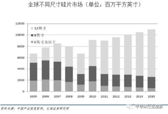
After that, pass 2 inches, 3 inches, and 4 inches. Next 5 inches, 6 inches, 8 inches, and then 12 inches. It is generally accepted in the industry that 4-inch silicon wafers dominated the mainstream in the 1980s, 6-inches dominated the 1990s, and 8-inches dominated the 2000s. In 2002, Intel and IBM first built a 12-inch production line, which had already accounted for it in 2005. 20%, and 30% in 2008, when 8 inches has dropped to 54% and 6 inches has dropped to 11%. It is estimated that around 2020, 18-inch (450mm) silicon wafers will begin to be put into use.
The development history of semiconductor wafer size
Monocrystalline silicon wafers are the raw material for the manufacture of semiconductor silicon devices, which are used to make high-power rectifiers, high-power transistors, diodes, switching devices, etc. Its follow-up products, integrated circuits and semiconductor discrete devices, have been widely used in various fields. As an important semiconductor material, monocrystalline silicon has been widely used in photoelectric conversion and traditional semiconductor devices. Light-emitting light sources driven by electricity, such as discharge lamps, fluorescent lamps or cathode ray light-emitting screens, light-emitting diodes, etc. From the perspective of information, technologies and components such as light emission, amplification, modulation, processing, storage, measurement, and display can be used to form an optoelectronic system with specific functions. For example, the use of optical fiber communication can achieve the purpose of rapid and large-capacity information transmission. It greatly improves the original similar technical level.
Production process flow of semiconductor monocrystalline silicon wafer
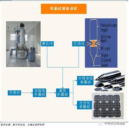
Monocrystalline silicon wafers are cut from monocrystalline silicon rods through a series of processes. The methods for preparing monocrystalline silicon include Czochralski method (CZ method), zone melting method (FZ method) and epitaxial method. The melting method is used to prepare monocrystalline silicon rods. The greatest demand for zone-melted silicon single crystals comes from power semiconductor devices.
Single crystal silicon preparation process
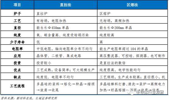
Czochralski method is abbreviated as CZ method. The characteristic of the CZ method is that it is integrated in a straight-tube heat system, heated by graphite resistance, melted the polysilicon contained in a high-purity quartz crucible, and then inserted the seed crystal into the surface of the melt for welding, while rotating the seed crystal, and then inverted In the crucible, the seed crystal is slowly raised upward, and the single crystal silicon is obtained through the processes of seeding, enlargement, shoulder rotation, equal diameter growth, and finishing.
The zone melting method is a method of using polycrystalline ingots to melt in regions and grow crystalline semiconductor crystals. Heat energy is used to generate a molten zone at one end of the semiconductor bar, and then the single crystal seed crystal is welded. Adjust the temperature so that the molten zone slowly moves to the other end of the rod. Through the entire rod, it grows into a single crystal with the same crystal orientation as the seed crystal. Zone melting method is divided into two types: horizontal zone melting method and vertical suspension zone melting method. The former is mainly used for the purification and single crystal growth of materials such as germanium and GaAs. The latter is in an atmosphere or vacuum furnace chamber, using a high-frequency coil to generate a molten zone at the contact between a single crystal seed crystal and a polycrystalline silicon rod suspended above it, and then move the molten zone upward for single crystal growth. Since the silicon melt is completely dependent on its surface tension and high-frequency electromagnetic force, it is suspended between the polycrystalline rod and the single crystal, so it is called the suspension zone melting method.
Comparison of Czochralski Method and Zone Melting Method
Monocrystalline silicon is purified from natural silicon raw materials to produce polycrystalline silicon, and then through zone melting or Czochralski method to produce zone melted or Czochralski monocrystalline silicon, and further form silicon wafers, polished wafers, epitaxial wafers, etc. The monocrystalline silicon grown by the Czochralski method is used to produce low-power integrated circuit components. The single crystal silicon grown by the zone melting method is mainly used in high-power electronic components. Czochralski processing technology: feeding → melting → necking growth → shoulder growth → equal diameter growth → tail growth, the grown crystal rod is raised to the upper furnace chamber and taken out after cooling for a period of time, which completes a growth cycle.
Suspended zone melting process: firstly fix the rod-shaped polycrystalline ingots accurately and vertically with clamps from the upper and lower axes. Use electron bombardment, high-frequency induction or optical focusing to melt a section of the area so that the liquid is supported by surface tension and does not fall. Move the sample or heater to move the melting zone. This method does not need a crucible and can avoid crucible pollution, so that very pure single crystals can be prepared, and this method can also be used for zone melting.
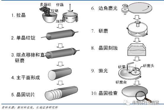
Semiconductor monocrystalline silicon wafer processing process
The demand for silicon in industrial production mainly comes from two aspects: semiconductor level and photovoltaic level. There are some differences in the processing process between semiconductor-grade monocrystalline silicon and photovoltaic-grade monocrystalline silicon. The purity of semiconductor-grade monocrystalline silicon is much higher than that of photovoltaic-grade monocrystalline silicon. The processing process of semiconductor-grade single crystal silicon wafers: single crystal growth→cutting→outer diameter barrel grinding→flat edge or V-groove treatment→slicing, chamfering→grinding, etching→polishing→cleaning→packaging.

Semiconductor monocrystalline silicon wafer cutting process flow
Analysis of Monocrystalline Wafer Industry Chain
The preparation process of monocrystalline silicon is different, and the purity and performance of the obtained products are very different, so the downstream application fields are also different. Monocrystalline silicon is an indispensable basic material in modern science and technology such as electronic computers and automatic control systems in daily life. TVs, computers, mobile phones, and automobiles are inseparable from monocrystalline silicon materials. As one of the popular materials for scientific and technological applications, monocrystalline silicon has penetrated into every corner of people's lives.

Monocrystalline silicon and its application classification
The entire monocrystalline silicon industry chain is relatively long, from the most upstream polycrystalline silicon raw materials and equipment, to the midstream monocrystalline silicon wafers, and extending to downstream power electronic devices, high-efficiency solar photovoltaic cells, radio frequency devices and microelectronic mechanical systems. , Various detectors and sensors, and finally to major industries such as computers, automobiles, and photovoltaics. Japan's Shin-Etsu Chemical and SUMCO have occupied an important market position in the field of monocrystalline silicon wafers.
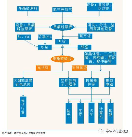
Panorama of the monocrystalline silicon industry chain
(1) Raw material pattern of upstream equipment
The monocrystalline silicon wafers used in semiconductor components are produced using polycrystalline silicon raw materials and then through single crystal growth technology. Crystalline silicon is a form of elemental silicon. When molten elemental silicon is solidified under supercooling conditions, silicon atoms are arranged in the form of diamond lattice into many crystal nuclei, such as these crystal nuclei grow into crystal grains with different crystal plane orientations. The crystal formed by these crystal grains is called polysilicon.
The raw material used in polysilicon comes from silica sand (silica), using hydrochloric acid (or chlorine, hydrogen) and metallurgical grade industrial silicon as raw materials, and synthesizing crude silicon (industrial silicon) powder and hydrochloric acid into trichlorosilane at high temperature, and then The trichlorosilane is chemically refined and purified, and then the trichlorosilane is subjected to multi-stage rectification to achieve a purity of more than 9 9s. The total content of metal impurities should be reduced to less than 0.1 ppba, and finally in a reduction furnace at 1050 Using ultra-high-purity hydrogen to reduce the trichlorosilane on the silicon core at ℃ to grow into high-purity polycrystalline silicon rods, monocrystalline silicon wafers are produced through single crystal growth technology.
The difference between electronic grade polysilicon (used to prepare semiconductor monocrystalline silicon) and solar grade polysilicon is mainly in the control of purity, the most obvious is in the distillation process, the height and quantity of the electronic grade and solar grade are very different. The purity of solar energy polysilicon is 6 decimal places, and the electronic grade polysilicon has 12 decimal places. 9. The entire process flow of electronic grade is higher than that of solar grade in raw material purity, pipeline cleaning, purification tower, and plant cleanliness.

Electronic grade polysilicon grade and related technical requirements
Compared with solar-grade polysilicon, the production of electronic grade polysilicon materials has very strict requirements on product purity and impurity control. The separation and purification process of chlorosilane is a key step in this process. The removal of boron by trichlorosilane has always been a technical bottleneck in the field of domestic electronic grade polysilicon materials.

The difference between electronic grade polysilicon and solar grade polysilicon
In recent years, with the rapid development of consumer electronics and the large demand for future automobiles, the global demand for electronic grade polysilicon materials has been steadily. It is expected that the consumption of silicon wafers will maintain the current upward trend in the next few years.
Global demand for electronic silicon materials
(2) All key production equipment comes from abroad
The process of processing monocrystalline silicon rods into monocrystalline silicon polished silicon wafers: single crystal growth→cutting→outer diameter rolling→flat edge or V-groove treatment→slicing, chamfering→grinding, etching→polishing→cleaning→packaging . Usually a production line requires the following equipment configuration. Although domestically-made equipment has covered all aspects of the production line, it is far from imported equipment in terms of quality and accuracy. Therefore, domestic monocrystalline silicon manufacturers currently use imported equipment for production.

Single crystal silicon production line equipment configuration
Single crystal furnace is a kind of equipment that uses graphite heater to melt polycrystalline silicon and other polycrystalline materials in an inert gas (nitrogen and helium) environment, and grows dislocation-free single crystals by the Czochralski method. There are two naming methods for monocrystalline silicon furnace models, one is the feeding amount and the other is the furnace chamber diameter. For example, models such as 120 and 150 are determined by the feeding amount, while the 85 furnace refers to the diameter of the main furnace barrel. The main body of the monocrystalline silicon furnace is composed of three parts: the host, the heating power supply and the computer control system.
Semiconductor materials are different from the general electronics industry. Not only are the purity and impurity specifications quite high, but even the source of raw materials and the production process of synthetic manufacturing must fully comply with the requirements of semiconductor manufacturers before they have the opportunity to enter the supply. system.
Furthermore, when material suppliers and semiconductor manufacturers are developing advanced process technologies, materials manufacturers have to keep pace with and respond to the results of process parameter adjustments. Although domestic material factories have the advantage of nearby assistance and supply, the degree of coordination and efficiency is not good. Not as good as an international manufacturer.

Cash products of major domestic and foreign monocrystalline silicon furnace manufacturers
(3) Global pattern of semiconductor wafers
The latest statistics from the International Semiconductor Industry Association (SEMI) show that the global silicon wafer shipment area in the third quarter of 2016 once again broke the historical record, reaching 2.730 billion square inches. Compared with the 2.706 billion square inches in the previous quarter, the shipment area in the third quarter increased by 0.9%, which was also an increase of 5.4% from the 2.591 billion square inches in the third quarter of 2015. Silicon wafers are the basic material for manufacturing semiconductor devices, and are very important materials for all electronic products such as computers, communications, and consumer electronics. The continuous growth of its shipment area also shows that the market's demand for electronic products is still growing.
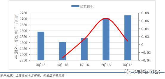
The global silicon wafer shipment area continues to rise in the past five quarters
The scale of the global silicon wafer market has steadily increased in recent years, and the future rise will become the main trend. Based on process standards, semiconductor materials can be divided into wafer manufacturing materials and packaging materials. In 2015, the overall wafer manufacturing market reached USD 24.1 billion, and the packaging materials market reached USD 19.3 billion. In 2015, the global semiconductor monocrystalline silicon market output value reached 43.4 billion U.S. dollars, accounting for 13% of the entire semiconductor industry.
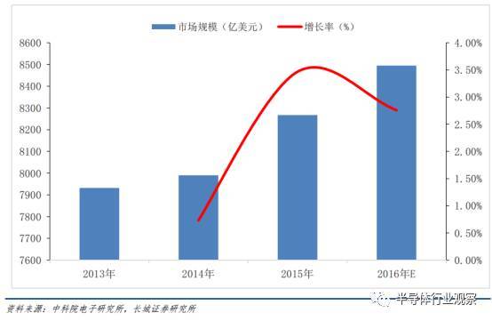
2013-2016 global silicon wafer market size
Semiconductor materials are divided into wafer manufacturing materials and packaging materials. Wafer manufacturing materials mainly include large silicon wafers, photoresist, wet chemicals, special gases, polishing fluids, and polishing pads. Silicon wafers and silicon substrates are the most important part of semiconductor materials, accounting for 32% of the market share of semiconductor materials. Due to the late start of my country’s semiconductor industry and the extremely high requirements for the preparation process of semiconductor silicon wafers, this part of the market is almost uniform. Monopolized by foreign manufacturers.
At present, a global oligopoly in the mainstream semiconductor wafer market has been formed. The six major wafer companies controlled by capital from Japan, Taiwan, Germany, and South Korea account for 95% of their sales. Shin-Etsu Chemical Industry Co., Ltd., as one of the leading companies in the semiconductor material industry in Japan, is the world's largest supplier of semiconductor wafers. In 2015, it accounted for 27% of the global semiconductor wafer market, followed by SUMCO.

The silicon wafer industry is almost monopolized by foreign manufacturers
The downstream market for semiconductor monocrystalline silicon wafers has broad prospects
The downstream market for semiconductor monocrystalline silicon wafers is generally improving and continues to grow. In 2015, the global semiconductor foundry market grew by 4.4%, reaching 48.8 billion U.S. dollars. In the context of the gradual rise of new technologies (cloud computing, artificial intelligence, and intelligent driving), the demand for in-depth big data processing has increased significantly, which will bring about rapid updates and upgrades of semiconductor hardware equipment. The semiconductor industry may usher in large-scale development opportunities.
Silicon wafers are the most important semiconductor material. Over the years, the market sales of silicon wafers have accounted for 32%-40% of the total sales of the entire semiconductor materials market. In recent years, the proportion of silicon wafers in the semiconductor materials market has basically remained stable. In 2013, silicon wafers accounted for 35% of the semiconductor materials market, and in 2015 it accounted for 34%. It is foreseeable that in the next few years, silicon wafers will still occupy an important position in the semiconductor materials market.
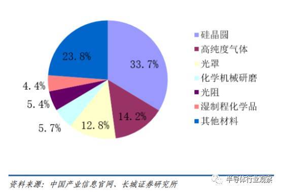
The proportion of the global semiconductor front-end materials market in 2015
According to the data, the total of polished silicon wafers and silicon epitaxial wafers in 2015 was 10434 MSI (million square inches); the SEMI Association stated that the total shipments of silicon wafers in 2015 surpassed the historical record set in 2014, and are expected to be in 2016 and 2017 It is expected to reach a new high this year.

Global silicon wafer shipments from 2013 to 2017
Although the market data of silicon wafers of different sizes fluctuated between 2005 and 2010, from 2011 to 2015, the scale of the global silicon wafer market of different sizes has steadily increased. It is estimated that the total amount of silicon wafers in 2017 will exceed 12 billion square inches, while the proportion of 12-inch silicon wafers is increasing, firmly occupying the mainstream position.
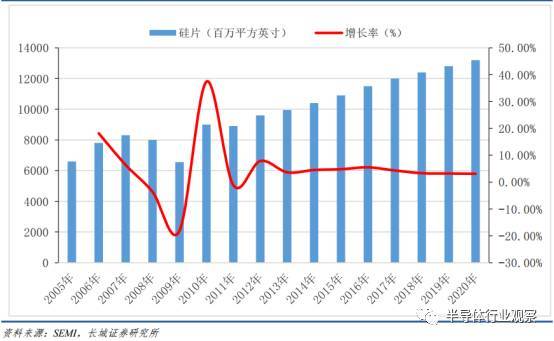
Global silicon wafer market status and development forecast
The slow growth of the global semiconductor market in 2015 was mainly because the 3.9% growth in the Asia-Pacific region offset the 10.3% decline in Japan and the 8.2% decline in Europe. Semiconductor demand is mainly affected by the slowdown in PC shipments, the appreciation of the US dollar, the shrinking Japanese economy, the European crisis and the Chinese stock market. Among them, China's semiconductor sales account for more than 50% of global semiconductor consumption. In the next few years, the global semiconductor market will show a trend of recovery, with growth of 1.4% and 3.1% in 2016 and 2017, respectively.
So far, the major semiconductor market in the Asia-Pacific region has promoted the growth of the semiconductor industry; in view of the weak Chinese economy, the semiconductor market will show a slow growth trend. In 2017, the global semiconductor market will show a momentum of growth, which will directly drive the growth of the global semiconductor silicon wafer market. Although the growth rate has slowed down, the growth trend is certain.
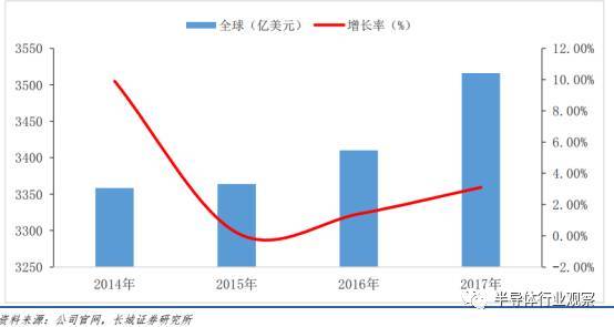
Global semiconductor market size in 2014-2017
As the destocking of the semiconductor industry is nearing completion, as market demand gradually picks up, the semiconductor industry's prosperity is gradually improving. It is expected that the global semiconductor capital expenditure and equipment investment scale can maintain a relatively stable growth rate in the next two years, and the semiconductor-grade silicon wafer industry will also benefit from this, and the demand for silicon wafers will rise steadily in the future.
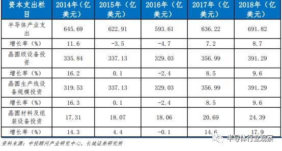
2014-2018 global semiconductor capital expenditures and
One point that needs to be emphasized is that the demand for 300mm silicon wafers continues to grow.
Semiconductor chip manufacturing technology follows Moore's Law. With the growth and development of the market for silicon wafers of different sizes, the overall development of silicon wafers follows the trend of large sizes. The larger the diameter of the monocrystalline silicon wafer, the more integrated circuits that can be carved, and the lower the cost of the chip. 300mm silicon wafers quickly entered the market from the end of the 1990s. After several years of development, they quickly became the mainstream of the market and will occupy the mainstream in the future.
According to market news released by SEMI, the global silicon wafer material market consumed approximately 10 billion square inches in 2015. Among them, 300mm accounts for about 70%. At the same time, shipments of 200mm silicon wafers currently occupy approximately 20% of the market share. As products such as MEMS and power simulation are expected to continue to develop beyond Moore's Law, 200mm silicon wafers will continue to maintain a certain market share in the future. The current industry’s mainstream forecast is that 450mm silicon wafers may be introduced into small-batch production around 2017, and Intel may only be the first batch of customers. In the next few years, 450mm silicon wafers will also follow the law and usher in a period of strong growth. The demand for silicon wafers is expected to continue to grow.
300mmFabs will reach a peak around 2021, after which the market will usher in a supplement of 450mmFabs, and 300mmFabs will gradually decrease. The overall supply is not expected to decrease.
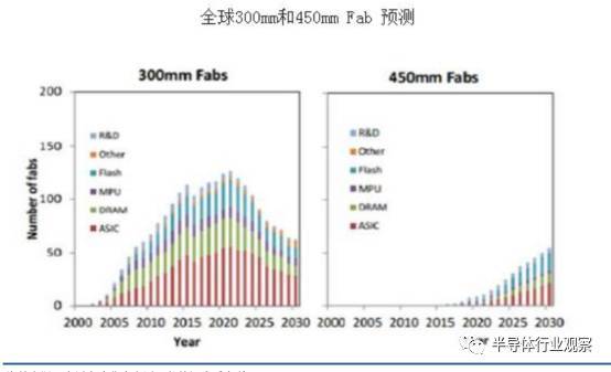
According to the 2016-2020 global wafer production capacity report from IC Insights, the number of 12-inch (300mm) wafer fabs in global operations continues to grow, and is expected to reach 100 in 2016. In addition, there are currently 8 12-inch fabs in the world that are expected to open in 2017, which may make this year the second year with the largest number of fabs in operation since 9 fabs started operations in 2014. By the end of 2020, it is expected that there will be another 22 12-inch fabs operating globally, bringing the total number of 12-inch fabs used in IC production globally to 117.
And if 18-inch (450mm) wafers enter mass production, the peak number of 12-inch fabs can reach about 125. 12-inch (300mm) silicon chips are mainly used for logic chips and memory chips, while the rest, such as automotive semiconductors, fingerprint recognition chips, and camera CIS chips, all use 8-inch silicon chips. According to the latest report of the research institute IC Insights, the compound annual growth rate (CAGR) of DRAM and NAND flash memory will reach 7.3% in the next five years, and the output value will increase from 77.3 billion US dollars last year to 109.9 billion US dollars. 42.2%. Therefore, the global demand for large 300mm silicon wafers will continue to expand.

According to statistics, mainland China has 10 12-inch wafer fabs. If all of them are put into production, the total production capacity of mainland China's 12-inch chips is expected to exceed 550,000 pieces per month. At present, the domestic output of 12-inch (300mm) silicon wafers is almost zero, which is the most scarce link in the industry chain. Japan produces the most 12-inch silicon wafers in the world, Shin-Etsu and SUMCO, whose combined production capacity and actual supply account for more than 2/3 of the world. The 300mm semiconductor-level large silicon wafer is not only an important link missing in the industrial chain, but also a need for the development of national security strategies. Therefore, the mainland's downstream demand for 12-inch silicon wafers is rapidly expanding.
In 2015, the global silicon wafer material market of different sizes consumed more than 10 billion square inches. It is expected that by 2020, the global silicon wafer material market consumption of different sizes will exceed 12 billion square inches. Among them, the 12-inch (300mm) wafer market will continue to expand and will account for 80% by 2020, while the 8-inch (200mm) and 6-inch (150mm) and below wafer market will become smaller and smaller.
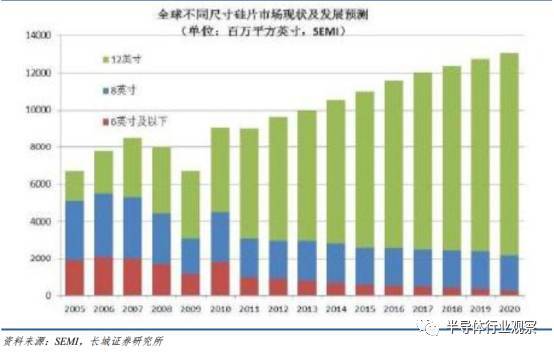
The current status and forecast of the global silicon wafer market of different sizes
COPYRIGHT @2021 Zhejiang Morinaga Optical & Electronic Equipment Co., Ltd. All rights reserved
浙ICP备11065660号-2

